Circuit diagram of 2 input ttl nand gate 2 input ttl nand gate circuit Ttl nand gate circuit diagram
74HC00 / 74HCT00, Quad 2 - Input TTL NAND Gate. Pinout Diagram « Funny
What is transistor transistor logic (ttl) circuit? Ttl integrated nand Electronic – ttl logic gate resistor values – valuable tech notes
Ttl circuit: transistor -transistor logic circuit operation
3 input ttl nand gate circuitWorking principle of the two-input ttl nand gate [diagram] circuit diagram using nand gate2 input nand gate circuit diagram.
Transistor-transistor logic : circuit, working & its applicationsTtl gate nand explain transistors Two input ttl nand gateSolved: figure shows a two-input ttl nand gate. the transistors.

Nand gate diagram 74hc00 ttl input quad 7400 pinout latch using gates nor push pull funny four has
2 input nand gate layoutLooking inside a vintage soviet ttl logic integrated circuit Not gate using nand gateA 4-input ttl nand gate and its circuit symbol.
A ttl 2-input nand gate breadboard circuit.Electronic – input and output impedance of a ttl nand gate – valuable Solved for ttl nand gate circuit shown in the figure. 1Ttl inverter diagram.

Circuit diagram of two input ttl nand gate
Draw the circuit diagram of ttl nand gate and explain its working withQ4) the circuit diagram of a ttl nand gate is illustrated with a set of Nand ttl transistorsTtl nand gate circuit diagram.
Circuit diagram of two input ttl nand gateCircuit diagram of 2 input ttl nand gate Solved a design of a digital logic circuit consists of 44What is transistor-to-transistor logic (ttl)? definition from techtarget.

Why does the ttl family use a totem pole circuit on the output
74hc00 / 74hct00, quad 2Why does the ttl nand gate use a 4 transistor design instead of 2 [diagram] ladder logic diagram nand gateTtl or gate circuit diagram.
What is transistor transistor logic (ttl) circuit? .


Solved For TTL NAND gate circuit shown in the figure. 1 | Chegg.com
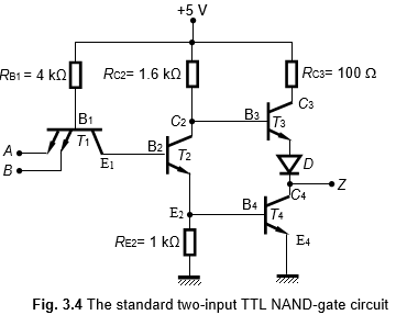
Working Principle of the Two-Input TTL NAND Gate

Electronic – TTL Logic Gate Resistor Values – Valuable Tech Notes

What Is Transistor-to-Transistor Logic (TTL)? Definition from TechTarget
![[DIAGRAM] Circuit Diagram Using Nand Gate - MYDIAGRAM.ONLINE](https://i2.wp.com/www.allaboutcircuits.com/uploads/articles/pinout-diagram-for-4011-quad-NAND-gate.jpg)
[DIAGRAM] Circuit Diagram Using Nand Gate - MYDIAGRAM.ONLINE

Transistor-Transistor Logic : Circuit, Working & Its Applications

Two input TTL Nand Gate | ECT 203 Logic Circuit Design| Module 5 - YouTube

3 Input Ttl Nand Gate Circuit - Circuit Diagram